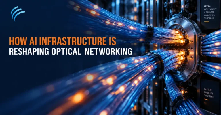
The scale of modern AI clusters has turned optical networking from a background infrastructure layer into one of the most closely watched supply chains in the industry. AI data centers require enormously more optical interconnect per unit of compute than previous generations of general-purpose data centers, and that demand is reshaping transceiver speeds, deployment volumes, and the underlying photonics architecture itself, all at a pace the optical supply chain is still working to keep up with.
800G Is Now the Default, 1.6T Is Entering Volume Production
800G pluggable optical transceivers have become the standard choice for new AI data center buildouts, with industry tracking showing the share of shipments at 800G and above rising sharply through 2026 to become the clear majority of new deployments. At the same time, 1.6T transceivers are moving from early samples into genuine volume production during 2026, enabled by the maturation of 200-gigabit-per-lane laser technology that doubles the per-lane rate used in 800G modules. Large hyperscalers are already qualifying 1.6T modules for next-generation AI clusters, with industry forecasts for 1.6T shipment volumes in 2026 ranging from several million to tens of millions of units depending on how quickly the underlying component ecosystem matures.

| Generation | Status in 2026 | Primary Driver |
| 400G | Mature, still cost-effective for general-purpose workloads | Legacy and non-AI-specific data center deployments |
| 800G | Default for new AI cluster buildouts | Hyperscaler AI training and inference cluster scale-out |
| 1.6T | Entering volume production | Next-generation AI clusters, enabled by 200G-per-lane lasers |
| 3.2T | Early development | Anticipated for AI clusters from roughly 2029 |
Why AI Workloads Consume So Many More Optical Ports
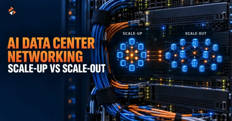
The ratio of optical transceivers to AI accelerators has risen substantially compared to earlier data center generations, with industry estimates now describing ratios of several transceivers per high-end AI chip, and considerably higher in some large ASIC-based training clusters. That’s a direct consequence of the scale-out networking architecture AI clusters depend on: connecting thousands of accelerators across many racks into a single coordinated training job requires proportionally more optical links than a traditional data center topology optimised for more modest east-west traffic. This dynamic is the core reason optical component demand has become a genuine constraint on how fast AI infrastructure can be built, not just a cost line item to manage.
Co-Packaged Optics: Moving the Optical Engine Closer to the Chip
Co-packaged optics, integrating the optical engine directly into the same package as the switch ASIC rather than connecting them via a separate pluggable module and printed circuit board traces, is the next major architectural shift in AI-driven optical networking. The appeal is substantial: CPO implementations claim meaningfully lower power consumption per port than conventional pluggable optics, along with higher achievable bandwidth density, both of which matter enormously as AI cluster power budgets become an increasingly binding constraint on how much compute a given facility can actually deploy. CPO remains an earlier-stage technology relative to pluggable optics, with 2026 broadly regarded across the industry as an early deployment year rather than the point of mainstream adoption, and the transition is expected to unfold gradually over the next several years as the supporting ecosystem, standards, and manufacturing capacity mature alongside it.
The Supply Chain Bottleneck Behind the Headline Numbers
The component most frequently identified as the binding constraint on optical transceiver supply is the electro-absorption modulated laser, the light source at the core of every 800G and 1.6T module, which requires high-precision Indium Phosphide fabrication that only a limited number of manufacturers worldwide can produce at the necessary quality and volume. Industry analysis has projected that transceiver production could fall meaningfully short of demand through the back half of this decade specifically because of this laser supply constraint, rather than any broader manufacturing capacity limit. For any organisation planning a large AI infrastructure buildout, this supply dynamic is worth factoring into procurement timelines directly: optical transceivers, historically a comparatively commoditised and readily available component, have become a genuine lead-time and allocation risk in a way that wasn’t true for previous data center generations.
What This Means for Overall AI Infrastructure Cost
Optical networking’s share of total AI data center capital cost has grown substantially compared to earlier data center generations, reflecting both the higher per-port cost of 800G and 1.6T optics relative to older transceiver generations, and the much larger number of optical ports each AI cluster requires. Industry tracking has shown optical spending rising as a proportion of total hyperscaler capital expenditure, a trend that’s expected to continue as 1.6T adoption scales and co-packaged optics moves toward broader deployment. For infrastructure planners, this means optical networking increasingly deserves the same level of dedicated cost modelling and procurement attention traditionally reserved for the accelerators themselves, rather than being treated as a comparatively minor line item within the broader cluster build.
Silicon Photonics as a Parallel Efficiency Path
Alongside the shift toward higher transceiver speeds and co-packaged optics, silicon photonics, manufacturing optical components using semiconductor fabrication techniques rather than traditional discrete optical assembly, is gaining adoption as a way to reduce both power consumption and per-unit cost. Silicon photonics implementations have demonstrated meaningful power efficiency gains and cost reductions relative to traditional optical component manufacturing, and the technology is increasingly viewed as complementary to, rather than competing with, the CPO transition, since silicon photonics manufacturing techniques are a natural fit for the tighter integration CPO requires. Together, these two trends, higher-speed transceivers moving toward co-packaged integration, and photonics manufacturing shifting toward semiconductor-style production, represent a broader industrialisation of optical networking that mirrors, in some respects, the manufacturing scale-up the semiconductor industry itself went through decades earlier.
What This Means for Infrastructure Planning Timelines
Given the combination of rapidly rising demand, a genuine component supply constraint, and a multi-year technology transition already underway toward CPO and silicon photonics, organisations planning AI infrastructure at meaningful scale benefit from engaging with optical vendors and component suppliers considerably earlier in the planning cycle than has historically been necessary for this layer of the data center stack. Treating optical networking procurement as a late-stage detail to finalise once compute and facility decisions are already locked in risks running directly into the lead-time and allocation pressures described above, at a point in the project timeline where there’s little flexibility left to adjust.
Explore more Digital Infrastructure analysis on TeckNexus — https://tecknexus.com/intelligence/digital-infrastructure-monthly-insights/.
Also check OTN Capacity & Right-Sizing Calculator and AI Data Center Interconnect (DCI) Bandwidth Planner